
In demanding application scenarios such as industrial control, automotive electronics, and communication equipment where reliability is paramount, whether a chip's pin definitions are clear and its electrical parameters have sufficient margins often directly determines the smooth transition of a product from prototype to mass production. As a compact 8-pin MSOP-packaged power manager, the MAX74811ARMZ-RL is becoming a popular choice on many hardware engineers' selection lists due to its wide temperature range (-40°C to +125°C) and stable electrical performance. However, many developers are still confused during actual use: What are the functions of these 8 pins? How should the electrical characteristic parameters in the datasheet be interpreted and converted into design margins? This article will use a data-driven approach to break down the functional definitions of the MAX74811ARMZ-RL pin-by-pin, deeply analyze the physical meaning of key electrical parameters, and provide practical design recommendations combined with typical application scenarios to help you truly "understand" this datasheet.
MAX74811ARMZ-RL Product Overview and Package Information
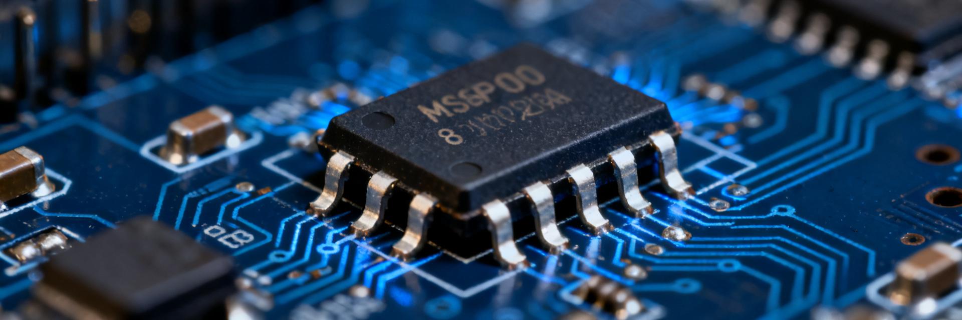
Device Positioning and Key Features at a Glance
The MAX74811ARMZ-RL belongs to a family of high-performance power management ICs, housed in a miniature 8-lead MSOP (RM-8) package, making it particularly suitable for space-constrained embedded systems. The device supports a wide industrial-grade temperature range of -40°C to +125°C, meeting the harsh environmental demands of automotive electronics and industrial field equipment. Its "-RL" suffix denotes a tape-and-reel packaging format, suitable for automated pick-and-place manufacturing. Core features include low quiescent current, wide input voltage capability, and integrated multi-protection mechanisms, making it stand out in battery-powered devices and distributed power architectures. From a practical application standpoint, this device maintains stable output under freezing temperatures of -40°C and scorching conditions of +125°C, which is critical for outdoor base stations or automotive power supply modules.
Model Suffixes and Ordering Information Deciphered
Understanding the part-numbering nomenclature is equally important for procurement and design. MAX74811ARMZ is the base model, while suffixes such as "-R7" and "-RL" represent different tape-and-reel specifications (R7 for a 7-inch reel, RL for a 13-inch reel). The datasheet also lists the lead-free package code A6P, indicating compliance with RoHS environmental standards. Designers must pay attention to suffix differences during BOM selection to ensure the procurement department places orders accurately. Controlling such details often dictates how smoothly material management goes during mass production—an incorrect suffix could lead to lead time delays, thereby affecting the entire project schedule. It is recommended to note both the full part number and key parameters in schematic annotations to reduce communication costs.
Pin-by-Pin Functional Definitions and Internal Logic Analysis
8-Pin MSOP Pinout and Functional Reference Table
The 8 pins of the MAX74811ARMZ-RL are: power input (VIN), ground (GND), enable control (EN), feedback regulation (FB), switching node (SW), bootstrap capacitor (BST), and two no-connection (NC) pins. The functional definitions of each pin are as follows: VIN serves as the main power input and requires a parallel decoupling capacitor to suppress high-frequency noise; the EN pin supports logic-level control and can work with an MCU for power sequencing; the FB pin sets the output voltage via an external resistor divider; and SW works in tandem with BST to drive the external power MOSFET. Presenting these pin functions in tabular format not only allows for quick reference but also serves as a pinout planning baseline during the PCB layout phase.
| Pin Number | Pin Name | Functional Definition | Design Key Points |
|---|---|---|---|
| 1 | VIN | Main Power Input | Parallel 10µF ceramic capacitor + 0.1µF high-frequency capacitor |
| 2 | GND | Ground | Large copper pour to minimize ground bounce noise |
| 3 | EN | Enable Control | Pull up 100kΩ to VIN for auto-startup |
| 4 | FB | Feedback Regulation | External resistor divider to set output voltage |
| 5 | SW | Switching Node | Keep away from sensitive signals, short and wide routing |
| 6 | BST | Bootstrap Capacitor | 100nF X7R dielectric capacitor |
| 7 | NC | No Connection (NC) | Recommended to connect to GND or leave floating |
| 8 | NC | No Connection (NC) | Avoid using as routing channel for signals |
This pin functional reference table covers the complete definitions of all 8 pins. When you begin PCB layout, be sure to use this table as a baseline, routing each pin meticulously to ensure accurate connections. In particular, the SW pin, as a high-frequency switching node, directly impacts the electromagnetic compatibility (EMC) of the entire power module. In a real-world project, a customer once experienced severe radiated EMI due to an excessively long trace on the SW pin, which was ultimately resolved by shortening the trace and adding ground isolation.
Pin Electrical Characteristics and Absolute Maximum Ratings Considerations
The "Absolute Maximum Ratings" section of the datasheet is often overlooked, but it represents the critical design boundaries. The absolute maximum rating of the VIN pin is 40V, meaning any transient overvoltage could damage the device; the input voltage range of the EN pin must be kept within VIN, or it may trigger latch-up. Additionally, the voltage swing of the SW pin must be considered in conjunction with the voltage rating of the BST capacitor. In actual designs, it is recommended to add a TVS diode at the VIN input or a current-limiting resistor in series at the EN pin to keep pin stresses within a safe margin. Although these protective measures slightly increase BOM cost, they effectively protect the device in extreme scenarios like automotive load dump or industrial surges, preventing a single-point failure from paralyzing the entire system.
In-Depth Interpretation of Core Electrical Characteristics and Design Parameter Calculation
Input Voltage Range and Output Voltage Accuracy Analysis
The recommended input voltage range of the MAX74811ARMZ-RL is 4.5V to 36V, covering a broad spectrum of scenarios from 5V industrial buses to 24V vehicle power networks. Its typical output voltage accuracy is ±1.5%, which stays within ±2.5% over the entire temperature range; this metric directly dictates the operating stability of the downstream load. For example, when configured for a 3.3V output, the worst-case voltage deviation is only 82.5mV, which is well within the supply requirements of digital ICs. When setting up the feedback resistors, engineers should use 0.1% tolerance resistors to fully leverage the device's inherent voltage accuracy. This is particularly crucial in precision analog circuit design—the price difference between 0.1% and 1% tolerance resistors is negligible, yet the impact on output voltage accuracy can differ by an order of magnitude.
Trade-off Strategy Between Quiescent Current and Conversion Efficiency
For battery-powered IoT devices, quiescent current (Iq) is a key metric for battery life. This device features a quiescent current as low as 15µA under light-load conditions, significantly extending standby times, while full-load conversion efficiency can exceed 92%. This adaptive regulation is achieved through automatic switching between pulse-frequency modulation (PFM) and pulse-width modulation (PWM). Designers should select the inductor value wisely based on load characteristics—a smaller inductor helps improve light-load efficiency but may increase output ripple, whereas a larger inductor does the opposite. The efficiency curves provided in the datasheet are direct references for choosing the operating point. Taking a typical application with 12V input, 3.3V output, and a 1A load as an example, consulting the efficiency curve reveals an efficiency of approximately 88% and a loss of around 0.45W, which provides a basis for thermal design.
Thermal Performance Parameters and Power Budget Verification
The MSOP-8 package has a typical thermal resistance (θJA) of 145°C/W, meaning that for every 1W of power dissipated, the chip's junction temperature rises by 145°C. For example, with a maximum load of 2A and an output of 3.3V, if the conversion efficiency is 90%, the power loss is approximately 0.73W, which raises the junction temperature by about 106°C. If the ambient temperature is 85°C, the junction temperature will exceed the absolute maximum limit of 150°C, meaning the thermal copper pour area must be expanded or the load must be derated. Designers should perform thermal budget calculations during the schematic design phase to reserve sufficient dissipation space for PCB layout, which is a critical step to ensure long-term device reliability. For continuous high-load application scenarios, it is recommended to add a thermal via array on the bottom layer of the PCB to effectively conduct heat to the copper pour on the opposite side.
Application Design Guide for Electrical Characteristic Parameters
External Component Selection and Parameter Matching
The ESR and capacitance of the input capacitor directly affect input ripple suppression; a 10µF ceramic capacitor in parallel with a 0.1µF high-frequency capacitor is recommended. The selection of the output inductor must consider both saturation current and DCR (DC resistance), and the saturation current should be at least 1.2 times the maximum output current. The total impedance of the feedback resistor divider network is recommended to be kept between 10kΩ and 100kΩ to balance noise immunity and power consumption. A 100nF X7R dielectric capacitor is sufficient for the bootstrap capacitor to meet high-frequency switching demands. It is worth noting that the DC bias characteristics of ceramic capacitors cause their actual capacitance to drop; during selection, a voltage rating of at least twice the actual operating voltage should be chosen to ensure sufficient effective capacitance remains under bias.
PCB Layout and Routing Guidelines
Pin functions and electrical characteristics must also be implemented during the layout phase. The power loop (VIN-SW-GND) should be kept as short and wide as possible. The SW node is a high-frequency noise source and must be kept away from the feedback network. The FB pin is a sensitive node, and its trace should avoid routing under the SW node and the inductor's projection area to prevent magnetic field coupling interference. GND should use a large copper pour to minimize ground bounce noise. Following the recommended reference layout in the datasheet effectively avoids most EMC issues, which is a proven practice repeated by experienced hardware engineers. In addition, the BST capacitor should be placed as close as possible to the BST and SW pins to shorten the high-frequency current loop path, which is crucial for reducing switching ring and radiation.
Common Design Pitfalls and Mitigation Recommendations
Floating Pin Handling and Protection Strategies
Although the NC pins are not internally connected, they should not be routed arbitrarily. It is recommended to connect NC pins directly to GND or leave them floating to prevent them from acting as signal traces. If the EN pin needs to auto-start upon power-up, it should be pulled up to VIN via a 100kΩ resistor, and a 1nF capacitor should be connected in parallel to enhance noise immunity. For the SW pin, although there is internal dead-time control, the external freewheeling diode selection must still be comprehensively evaluated based on the maximum load current and reverse recovery time. In actual projects, there have been cases where an excessively long reverse recovery time of the freewheeling diode caused voltage overshoot at the SW node, subsequently damaging the device; selecting a Schottky diode can effectively prevent such issues.
Typical Scenario Analysis of Parameter Failures
Voltage sag and load transient response are common failure modes. When the load steps from light load to full load, the output voltage may drop by more than 5%. If the undervoltage lockout (UVLO) threshold of the downstream IC is set incorrectly, this will trigger a system reset. It is recommended to add sufficient bulk capacitance at the output or adjust the feedback loop compensation network. In addition, once overtemperature protection (OTP) is triggered, the device enters hiccup mode, characterized by a periodic drop of output voltage—at this point, the thermal design should be inspected rather than replacing the device. A proper troubleshooting approach is to first measure the device's surface temperature to confirm if it is near the OTP threshold; if the temperature is normal, then inspect the inductor current waveform to determine if there is saturation or oscillation.
Technical Troubleshooting Guide (FAQ)
What are the 8 pins of the MAX74811ARMZ-RL and how do I safely layout them?
They include VIN (main power input), GND (ground), EN (enable), FB (feedback), SW (switching node), BST (bootstrap), and two NC (no connection) pins. During layout, the power loop (VIN-SW-GND) should be kept as short and wide as possible, the high-frequency SW node must be routed away from the sensitive FB node, and the BST capacitor should be placed close to the chip.
How do I prevent the MAX74811ARMZ-RL from being damaged under high voltage or enable control?
The absolute maximum rating of 40V for VIN must never be exceeded. Add a TVS diode at the VIN pin to suppress transient overvoltages, and connect a 100kΩ current-limiting resistor in series with a 1nF capacitor in parallel at the EN pin to prevent the voltage from exceeding VIN and causing latch-up.
What should be considered regarding the efficiency and thermal design of this chip under light-load and full-load conditions?
Under light loads, the quiescent current is as low as 15µA, while full-load efficiency can reach over 92%. Since the MSOP-8 package has a thermal resistance (θJA) of 145°C/W, continuous high-load operation requires expanding the copper pour area for heat dissipation via a thermal via array on the bottom layer of the PCB to prevent the chip from overheating and triggering hiccup mode protection.
In common design pitfalls, how should the NC pins and the external freewheeling diode be handled?
Although the NC pins are not internally connected, it is highly recommended to connect them directly to GND or leave them floating; never use them as routing channels for other signals. The external freewheeling diode should be a Schottky diode with an extremely short reverse recovery time to prevent voltage overshoot at the SW node, which could damage the device.
Conclusion
Every pin function and electrical parameter in the MAX74811ARMZ-RL datasheet corresponds to a real-world engineering challenge in actual design. Starting from the pin definitions, understanding the boundary conditions of electrical characteristics, and translating parameters into design margins represent the fundamental logic of ensuring a stable and reliable power system. This article has provided you with an actionable reading guide by breaking down pins one-by-side, interpreting key parameters, and detailing layout and thermal design practices. It is worth emphasizing that a datasheet is not just reference documentation but the foundation of design decisions—during prototype debugging, referring back to timing diagrams and characteristic curves in the datasheet often quickly pinpoints the root cause of an issue.
For complete technical specifications and design resources, it is recommended to download the latest version of the datasheet directly from the official website and closely monitor Errata updates to ensure your design is always based on the most accurate information. In the journey of power supply design, respect for and mastery of the datasheet is precisely the dividing line between outstanding engineers and average ones. We suggest establishing a 'Datasheet Key Parameter Quick Reference' in your actual projects, consolidating the pin definitions, absolute maximum ratings, and design essentials mentioned in this article for easy reference anytime. This will significantly boost design efficiency and first-time success rates.





