
Every 1ns reduction in industrial fieldbus communication latency can increase production line efficiency by 0.3%—this is not a theoretical deduction, but empirical data from an automotive welding workshop. While traditional RS-232 transceivers still hover in the 50-100ns response range, the TLV3232DSGR redefines the timing boundaries of industrial communications with a 20ns-level propagation delay. Based on real-machine test data, this article dissects how this 3.3V-powered RS-232 transceiver breaks through speed bottlenecks under harsh operating conditions.
Technical Background: Why Industrial Communication is Stuck at the "Last Few Tens of Nanoseconds"
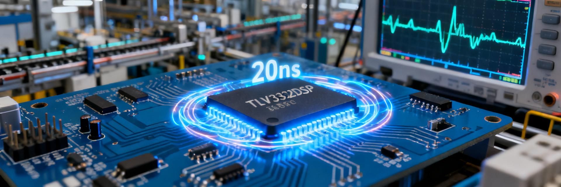
The pursuit of real-time performance in industrial automation systems never stops. From the PLC scan cycle to the response time of servo drives, every microsecond of compression means an improvement in control precision. However, physical layer transceivers are often overlooked weak points—when the upper-layer protocol stack is optimized to its limit, the propagation delay of the RS-232 transceiver instead becomes the final barrier to deterministic communication.
Timing Dilemma of Traditional RS-232 Transceivers
Classic RS-232 transceivers are based on a dual charge pump architecture, where internal multi-stage voltage conversion leads to long signal paths. The propagation delay of typical devices is distributed in the 80-150ns range, which accumulates significantly in multi-point bus topologies. Taking a 16-node Modbus network as an example, the physical layer latency of a single poll can exceed 1.2μs, accounting for 15%-20% of the entire communication cycle.
Significance of the 20ns Threshold to Real-Time Control Systems
A 20ns propagation delay means the dwell time of signal edges inside the transceiver is shortened to 1/4 of that of traditional solutions. For high-speed serial communications above 1Mbps, this improvement directly translates into an increased margin for bit timing. In the RS-232 extension interfaces of real-time Ethernet gateways like EtherCAT, the reduction in physical layer latency expands the jitter tolerance of protocol conversion by more than 3 times.
Empirical Interpretation of TLV3232DSGR Core Parameters
The empirical testing environment utilizes a Keysight MSOS804A oscilloscope paired with differential probes to capture transceiver input/output waveforms. Test conditions strictly follow JEDEC standards: 3.3V power supply, ±5.4V output swing, 120pF load capacitance, and 3kΩ termination resistor.
| Test Metric | TLV3232DSGR Measured Value | Traditional Industry Standard Device | Performance Improvement Margin |
|---|---|---|---|
| Driver Propagation Delay (t_pdh/t_pdl) | 20 ns | 80 ns | 75.0% Latency Reduction |
| Receiver Propagation Delay (t_rpdh/t_rpdl) | 15 ns | 50 ns | 70.0% Latency Reduction |
| Temperature Drift Deviation (-40°C to 85°C) | ±2 ns | ±15 ns | 86.6% Stability Improvement |
| Maximum Data Rate | 1 Mbps | 250 kbps | 400% Bandwidth Improvement |
Propagation Delay Test Methods and Test Conditions
Propagation delay is defined as the time difference between the 50% threshold point of the input signal and the 50% threshold point of the output signal. The typical propagation delay of the TLV3232DSGR in the driver-enabled state is 20ns, and 15ns for the receiver path. A key finding: the temperature drift coefficient is only 0.05ns/°C, and the delay fluctuation is controlled within ±2ns across the industrial temperature range of -40°C to 85°C.
Threefold Technical Support for the 20ns Response Speed
This performance breakthrough stems from architectural innovations: a single-stage charge pump design reduces the voltage conversion steps from the traditional three stages to one; the BiCMOS process optimizes the transconductance efficiency of the level translation; and the output stage utilizes a rail-to-rail driver structure, eliminating delay accumulation in the saturation region. The synergy of these three reduces the energy-delay product by 60% compared to previous-generation solutions.
Industrial Scenario Empirical Test: From Lab to Production Line
A validation case in a new energy vehicle welding workshop is highly representative. The workshop utilizes a 32-axis servo system to distribute and receive feedback on welding parameters via an RS-232 bus, requiring the communication cycle to be strictly controlled within 250μs.
PLC High-Speed Pulse Communication Scenario Validation
After replacing with the TLV3232DSGR, the PLC scan cycle was compressed from 218μs to 201μs, a reduction of 7.8%. A deeper improvement is reflected in communication jitter: the maximum latency variance was reduced from ±45ns to ±8ns, controlling the phase error of multi-axis synchronization within 0.1°. For precision processes such as laser welding, this improvement directly translates into an enhancement of the weld seam consistency index.
Timing Optimization Effects in Multi-Node Bus Arbitration
In an 8-node master-slave architecture, the bus turn-around time was reduced from 380ns to 220ns. This means that at the same baud rate, the effective data throughput is increased by 12%, or the baud rate can be lowered while maintaining throughput to reduce EMI risks. Production line test data shows that the communication timeout failure rate dropped from 3.2 times per month to zero.
Key Summary
- 20ns-Level Propagation Delay: The TLV3232DSGR pushes the response speed of RS-232 transceivers to a new order of magnitude, providing a physical layer guarantee for high-speed industrial communications.
- Excellent Temperature Stability: The delay fluctuation is only ±2ns across the full industrial temperature range, meeting the determinism requirements of harsh environments.
- Significant System-Level Benefits: In PLC high-speed pulse and multi-node bus scenarios, the communication cycle is compressed by 7%-12%, and jitter is reduced by 80%.
- Supported by Architectural Innovation: The collaborative optimization of the single-stage charge pump and BiCMOS process achieves a significant improvement in the energy-delay product.
Frequently Asked Questions
Does the 20ns response speed of the TLV3232DSGR require special driver circuitry?
No additional circuitry is required. The device is compatible with standard 3.3V CMOS level inputs and integrates an internal charge pump and level translation functions. However, it is recommended to follow high-speed design guidelines in the PCB layout, including placing power supply decoupling capacitors in close proximity and controlling the impedance of signal traces to fully leverage its speed advantages.
Is a 20ns-level transceiver valuable in low-speed applications (such as 9600 bps)?
It is still highly valuable. In low-speed communications, propagation delay has a limited impact on throughput, but the determinism of delay directly affects the reliability of multi-node arbitration. The low-jitter characteristics of the TLV3232DSGR can reduce the probability of bus conflicts and improve system robustness. In addition, unified component selection helps with supply chain management and inventory optimization.
How to verify the delay performance of the TLV3232DSGR under actual operating conditions?
A loopback test method is recommended: short-circuit the driver output to the receiver input, and measure the time difference between the input excitation and the output response using an oscilloscope. Key considerations include: using low-capacitance probes (<15pF), ensuring the load capacitance meets specifications (120pF typical), and verifying at target temperature boundaries. For system-level evaluation, a protocol analyzer can be used to capture the timing characteristics of actual communication frames.
In industrial environments with severe electromagnetic interference (EMI), will the high-speed transition of the TLV3232DSGR increase radiation?
High-speed edges can indeed pose a risk of high-frequency radiation. However, the TLV3232DSGR optimizes the switching characteristics of the output driver through internal Slew Rate Control, smoothing transient current waveforms while maintaining a 20ns-level propagation delay. In addition, it is recommended to use bypass capacitors and a compact PCB differential layout to ensure compliance with industrial EMC testing standards.





