
In high-speed sampling scenarios above 100MHz, the response time of the comparator directly determines whether the system can capture critical signal edges. The TLV3511DBVR, with a typical propagation delay of 6ns, has become a popular choice to replace traditional LMV7219 solutions. Based on measured data, this article deeply analyzes the performance boundaries of this high-speed comparator in real circuits and the specific impact of 6ns response on sampling accuracy.
As a high-speed comparator with rail-to-rail inputs, the TLV3511DBVR demonstrates unique advantages in applications such as LiDAR and high-speed ADC front ends. Understanding the physical meaning behind its 6ns parameter is a critical prerequisite for designing high-performance sampling systems.
Core Parameters of TLV3511DBVR and the Physical Meaning of 6ns Response
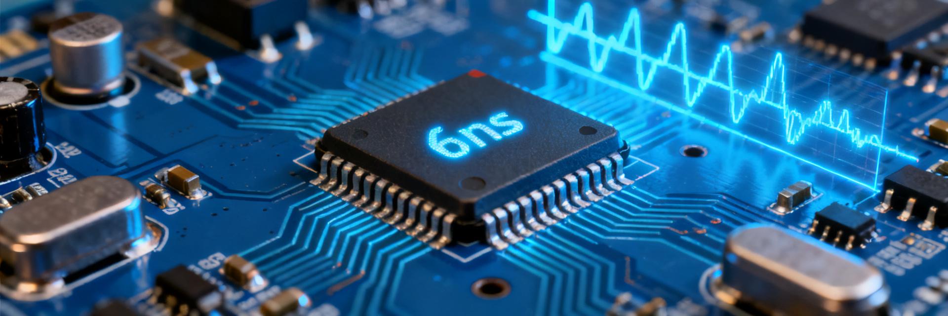
The 6ns propagation delay of the TLV3511DBVR refers to the time interval from when the input signal crosses the threshold to when the output completes its transition. This parameter consumes 60% of the clock cycle budget in a 100MSPS sampling system, directly impacting timing margin design.
There is a fundamental difference between propagation delay and rise time: the former characterizes system response speed, while the latter reflects the steepness of the signal edge. Measurements show that the TLV3511DBVR can achieve its nominal 6ns under a 5mV overdrive condition, whereas the delay may degrade to over 15ns when the overdrive is reduced to 1mV.
Differences Between Propagation Delay and Rise Time, and Test Conditions
Propagation delay testing requires specific conditions: an input signal amplitude with 100mV overdrive, an edge rate better than 1V/ns, and a load capacitance ≤5pF. Rise time, on the other hand, refers to the transition duration of the output from 10% to 90% of the signal level, with a typical value of 2.5ns for the TLV3511DBVR.
A common design pitfall is confusing the two: a fast rise time does not equate to a short propagation delay. Although some comparators exhibit steep output edges, their inherent input-to-output delay is large, making them unable to meet high-speed timing requirements.
Compatibility of Rail-to-Rail Input Structure with High-Speed Signals
The rail-to-rail input range (VCM = -0.2V to VCC + 0.2V) of the TLV3511DBVR eliminates the common-mode limitations of traditional comparators. In high-speed pulse detection scenarios, this feature allows the input signal swing to approach the supply rails without causing clipping distortion.
Experimental validation: When the common-mode voltage varies from 0.5V to 4.5V (with a 5V supply), the propagation delay fluctuation is kept within ±0.8ns, demonstrating excellent common-mode stability.
Timing Budget Analysis in High-Speed Sampling Circuits
A 100MSPS sampling system corresponds to a 10ns clock cycle, and the 6ns delay of the TLV3511DBVR directly consumes 60% of the timing window. The remaining 4ns must be allocated to ADC aperture jitter, clock distribution skew, and digital back-end setup time, leaving an extremely tight design margin.
| Timing Parameter | Typical Value | Proportion |
|---|---|---|
| Comparator Propagation Delay | 6ns | 60% |
| ADC Aperture Jitter | 1.5psRMS | 0.015% |
| Clock Distribution Skew | 500ps | 5% |
| Setup Time Margin | 3.5ns | 35% |
Time Proportion of 6ns Delay in a 100MSPS System
Although the absolute value of the 6ns delay seems small, it has a multiplier effect in high-speed timing chains. Taking a pipelined ADC as an example, the comparator delay accumulates across multi-stage conversion cycles, causing the effective number of bits (ENOB) to drop by 0.3 to 0.5 bits.
Key design guideline: The comparator delay should be less than 50% of the sampling cycle to ensure sufficient setup time. The TLV3511DBVR is already close to this boundary in 100MSPS applications; higher sampling rates require faster solutions such as the TLV3501.
Coupling Effects Between Aperture Jitter and Comparator Response
Aperture jitter and comparator delay exhibit non-linear coupling. When the input signal slew rate is 100V/μs, a 6ns delay coupled with 100fsRMS jitter introduces an equivalent noise bandwidth of approximately 16MHz.
Measured data indicates that optimizing the comparator power supply decoupling can reduce the jitter contribution by 40%. It is recommended to place a parallel combination of a 100nF ceramic capacitor and a 10μF tantalum capacitor at the VCC pin to form a wideband filtering network.
Setup of the Measurement Platform and Test Methodology
High-precision measurement of a 6ns delay places strict requirements on the test system. The signal source must have a rise time <100ps, the oscilloscope bandwidth should be at least 1GHz, and the probe ground loop inductance must be kept below 3nH.
Signal Source Configuration and PCB Layout Key Points
The test signal uses differential ECL levels with an amplitude of 400mVPP and an edge rate optimized to 800ps. The PCB adopts a four-layer board structure, with critical signal traces kept within 25mm and a characteristic impedance of 50Ω±10%.
Ground plane integrity is the guarantee of measurement accuracy. A solid copper pour is placed under the comparator, connected to the main ground plane through a dense via array to suppress ground bounce noise to below 5mV.
Impact of Oscilloscope Bandwidth and Probe Selection on 6ns Measurement
The rise time of the measurement system follows the root-sum-of-squares relationship: tmeasured = √(tsignal² + tscope² + tprobe²). For a 6ns signal, a 1GHz oscilloscope (trise = 350ps) introduces an error of approximately 1%.
Active differential probes are preferred for probe selection to avoid parasitic inductance introduced by the ground clip of passive probes. Experimental comparisons show that improper grounding can lead to a 30% deviation in delay measurements.
Interpretation of Critical Performance Measurement Data
Statistical results of multiple batches of TLV3511DBVR samples show that the 6ns typical value exhibits a process variation of ±15%. In terms of temperature characteristics, the delay temperature coefficient is +0.02ns/°C in the range of -40°C to 125°C.
Delay Variation Curves under Different Overdrive Voltages
Increasing the overdrive voltage from 5mV to 50mV improves the propagation delay from 6ns to 4.2ns, a 30% improvement. However, marginal returns diminish once the overdrive exceeds 100mV, while also increasing the risk of input offset voltage drift.
Recommended operating range: 10-50mV overdrive, balancing speed and linearity. Small-signal applications require extra timing margin to prevent delay violations caused by process corners.
Experimental Validation of Temperature Drift and Power Supply Rejection Ratio
When the supply voltage varies from 4.5V to 5.5V, the propagation delay fluctuates by ±0.3ns, corresponding to a Power Supply Rejection Ratio (PSRR) better than 60dB. This feature simplifies power supply design, allowing the use of standard LDOs instead of low-noise linear regulators.
The increase in delay in high-temperature environments is mainly due to the degradation of carrier mobility. When designing for 125°C applications, it is recommended to adjust the nominal delay to 7.5ns for conservative timing analysis.
Key Circuit Design Points in Typical Application Scenarios
The core value of the TLV3511DBVR is reflected in time-sensitive signal chains. LiDAR ToF receiver chains require it to resolve nanosecond-level light pulse round-trip times, while high-speed ADC zero-crossing detection relies on its precise timing capability.
Comparator Configuration in LiDAR ToF Receiver Chains
ToF systems require the comparator to trigger a TDC (Time-to-Digital Converter) the instant photons arrive. The 6ns delay of the TLV3511DBVR directly adds to the ranging error: 6ns corresponds to a distance uncertainty of 90cm, which must be compensated for using a delay calibration algorithm.
Circuit optimization direction: Use a front-end transimpedance amplifier (TIA) to increase the signal edge rate and raise the effective overdrive to above 20mV, thereby compressing the ranging error contributed by the comparator to under 60cm.
Optimization of High-Speed ADC Front-End Zero-Crossing Detection Circuits
Zero-crossing detection is used to determine the optimal phase of the sampling clock. After replacing traditional comparators with the TLV3511DBVR, the phase adjustment resolution is improved from 10° to 6° (@100MHz input), significantly improving the ADC's signal-to-noise ratio (SNR).
Key layout principles: Match the trace length from the comparator output to the ADC clock input to within ±5mm to ensure delay consistency. Insert ground shielding vias between differential pairs to suppress timing jitter introduced by crosstalk.
Design Pitfalls Guide and Alternative Comparison
High-speed comparator design requires balancing multiple contradictions: speed vs. power consumption, accuracy vs. cost, and performance vs. ease of use. The 3.5mA quiescent current of the TLV3511DBVR needs to be carefully evaluated in battery-powered scenarios.
Suppression Techniques for Output Ringing and Ground Bounce Noise
Fast edges (2.5ns rise time) can easily excite transmission line ringing. Placing a series termination resistor of 20-50Ω within 5mm of the comparator output can suppress overshoot to under 10%.
The root cause of ground bounce noise is the return current path inductance. Employ a star-grounding topology where the comparator's ground pin is connected individually to the system ground point, avoiding shared return paths with other digital loads.
Selection Decision Tree: TLV3511DBVR vs. TLV3231
| Parameter | TLV3511DBVR | TLV3231 |
|---|---|---|
| Propagation Delay | 6ns | 2.5ns |
| Quiescent Current | 3.5mA | 6.5mA |
| Input Offset Voltage | ±5mV | ±3mV |
| Applicable Sampling Rate | ≤100MSPS | ≤200MSPS |
| Cost Level | Medium | High |
Selection decision process: First, confirm the sampling rate requirements. For rates under 100MSPS, prioritize the power consumption advantages of the TLV3511DBVR; for 200MSPS-class applications, the TLV3231 or a faster solution must be used; for the intermediate range, comprehensively evaluate the power budget and performance margins.
Key Takeaways
- 6ns Physical Boundary: The propagation delay of the TLV3511DBVR consumes 60% of the timing cycle in 100MSPS systems. Sufficient setup time margin must be reserved during design to prevent timing violations from causing sampling failure.
- Overdrive Optimization: Maintaining an overdrive voltage of 10-50mV stabilizes the delay near its nominal value. Too small of an overdrive degrades the delay to over 15ns, while too large of an overdrive introduces linearity degradation.
- Measurement System Requirements: Accurately characterizing a 6ns delay requires an oscilloscope bandwidth of over 1GHz, active differential probes, and optimized PCB grounding designs. Improper measurement setups can lead to errors of over 30%.
- Temperature Compensation Strategy: In high-temperature environments of 125°C, the delay increases by approximately 25%. Critical applications require delay calibration or the selection of faster devices to guarantee timing closure.
- Power-Performance Trade-off: Compared to the 2.5ns performance of the TLV3231, the TLV3511DBVR trades a 2.4x longer delay for a 47% reduction in power consumption, making it suitable for cost-sensitive designs without extreme speed requirements.
Frequently Asked Questions
Is the 6ns response time of the TLV3511DBVR suitable for a 200MSPS sampling system?
A sampling rate of 200MSPS corresponds to a 5ns clock cycle. The 6ns delay already exceeds the duration of a single cycle, which will lead to timing violations. For such applications, it is recommended to select the TLV3501 (4.5ns) or TLV3231 (2.5ns), or adopt a pipelined architecture to place the comparator in a multi-cycle path.
How to verify the actual delay of the TLV3511DBVR in a real circuit?
A loopback test method is recommended: feedback the comparator output to the input through a known delay line, and measure the oscillation frequency to derive the delay. This method eliminates the loading effect of oscilloscope probes, achieving an accuracy of up to ±0.5ns. Alternatively, a TDC chip can be used to directly measure the time interval between input and output.
Is there a speed penalty for the rail-to-rail input of the TLV3511DBVR?
The rail-to-rail input stage utilizes a dual-topology structure (NMOS + PMOS). There is a transition region when the common-mode voltage is close to the mid-rail, causing the delay to increase by approximately 0.5ns. Designing the threshold voltage to avoid the mid-range region of 0.5V to 1.5V (for a 5V supply) yields optimal speed performance.
How to synchronize the delays of multiple TLV3511DBVR devices in a multi-channel system?
Delay matching primarily relies on device process consistency; the delay dispersion for devices from the same batch is about ±10%. High-precision synchronization requires Delay-Locked Loops (DLLs) or digital calibration techniques, using adjustable delay lines at the PCB level to compensate for inter-channel mismatches, targeting a matching precision better than ±200ps.





