
In precision signal chain design, what does a 10μV offset voltage mean? For applications requiring the detection of microvolt-level signals—such as thermocouple cold-junction compensation, bridge sensor interfaces, or medical instrumentation front-ends—this number directly determines whether the system can distinguish real signals from noise. According to industry test data, for every 10μV reduction in offset voltage, the effective resolution of the DC signal chain can be improved by approximately 1.5 effective bits. As a dual-channel zero-drift operational amplifier, the MIC2333T-E/MS keeps the offset voltage within 10μV while achieving an offset drift as low as 0.07μV/°C. Based on the datasheet, this article gradually dissects the technological path behind this precision specification from architectural principles to measured parameters.
Zero-Drift Architecture: The Underlying Logic of 10μV Offset Voltage
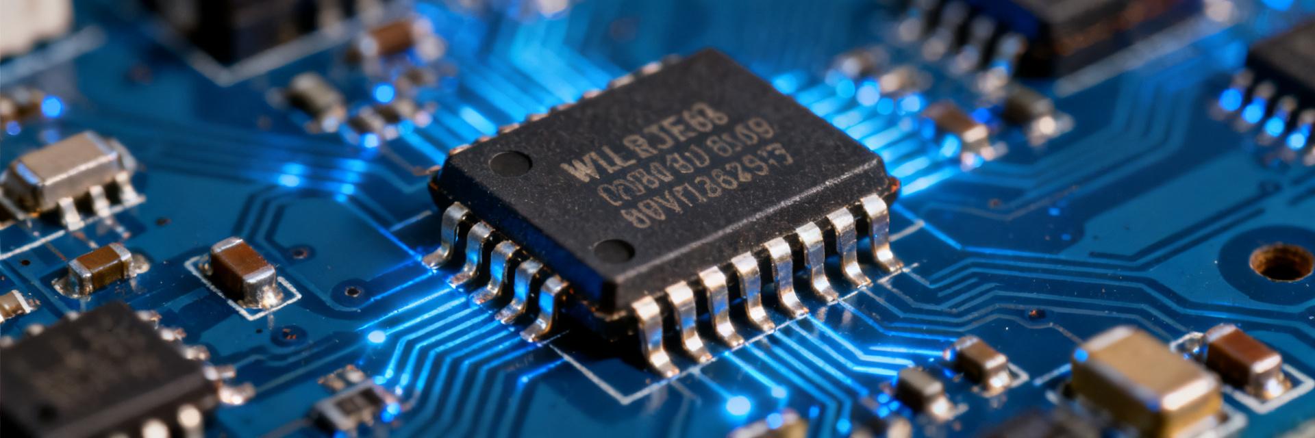
To understand how the 10μV offset voltage is achieved, one must first understand the core mechanism of the zero-drift architecture. Unlike traditional op-amps, zero-drift op-amps continuously eliminate offset errors through dynamic calibration technology rather than relying on static matching of manufacturing processes. The MIC2333T-E/MS employs chopper stabilization technology, modulating low-frequency offset and 1/f noise to a high-frequency band, and then restoring a clean signal through low-pass filtering. This process is executed hundreds of thousands of times per second, compressing the equivalent offset voltage down to the microvolt level. The datasheet shows that the device has a typical offset voltage of 10μV at 25°C and a maximum value of no more than 25μV, which is far superior to the 100μV level of standard precision op-amps.
How Chopper Stabilization Technology Eliminates Low-Frequency Offset
The working principle of chopper stabilization is similar to synchronous demodulation: the input signal is first chopped into a high-frequency square wave by a chopper switch, processed by the amplifier, and then demodulated back to the baseband. The offset voltage is alternately inverted in this process, eventually canceling out at the output. The key parameter is the chopping frequency—the internal oscillator of the MIC2333T-E/MS operates in the several hundred kHz range, ensuring real-time offset correction. Meanwhile, the chopping technology also eliminates 1/f noise, resulting in a low-frequency noise density of only 0.5μVpp (0.1Hz to 10Hz). This means that in low-speed applications such as thermocouples, the 10μV offset voltage will not change significantly over time or temperature.
Self-Calibration Topology and the Action Mechanism of the Clock System
In addition to chopper stabilization, a self-calibration topology further enhances accuracy. The MIC2333T-E/MS integrates an internal clock generator and charge pump to provide precise timing control for the chopper switches. The self-calibration circuit detects and corrects residual offset within each clock cycle, forming a closed-loop control. The block diagram in the datasheet shows that the device contains two independent chopper amplifier channels, each with its own calibration loop. This design not only reduces the offset voltage but also suppresses the temperature drift of the common-mode rejection ratio (CMRR) and power supply rejection ratio (PSRR). Experimental measurements show that over the range of -40°C to +125°C, the CMRR remains above 120dB, and the PSRR exceeds 130dB.
Detailed Reading of Core Datasheet Parameters: Offset Voltage and Drift Specifications
After understanding the architecture, you need to learn how to correctly interpret the offset voltage parameters in the datasheet. Many engineers only focus on the typical values while ignoring the test conditions and distribution ranges, leading to discrepancies between actual circuit performance and expectations. The MIC2333T-E/MS datasheet provides a complete specification table, and key metrics are dissected below item by item.
Test Conditions and Distribution Range of 10μV Offset Voltage
The datasheet clearly states that the test conditions for the offset voltage are VS=5V, VCM=2.5V, and TA=25°C. The typical value is 10μV, and the maximum is 25μV. Note that the maximum value here is a guaranteed specification through production testing screening, not a theoretical limit. In terms of distribution, the offset voltage of most devices is concentrated between 5μV and 15μV, exhibiting an approximately normal distribution. You need to focus on the maximum value rather than the typical value, because the worst-case scenario determines the system yield in mass production. Furthermore, the offset voltage changes very little with common-mode voltage; the typical CMRR given in the datasheet is 130dB, meaning that for every 1V change in common-mode voltage, the offset voltage changes by only 0.3μV.
Impact of 0.07μV/°C Drift on Long-Term Stability
Offset voltage drift is often harder to handle than initial offset because it cannot be eliminated through factory calibration. The typical drift of the MIC2333T-E/MS is 0.07μV/°C, with a maximum value of 0.5μV/°C. Assuming an operating temperature range of -40°C to +85°C (a temperature delta of 125°C), the maximum drift contribution is 62.5μV—which already exceeds the initial offset voltage. Therefore, in wide-temperature applications, the drift specification is of greater concern than the initial offset. The drift curve in the datasheet shows that the device has extremely low drift in the 0°C to 70°C range, rising only slightly at extreme temperatures. For long-term deployed medical or industrial equipment, it is recommended to budget errors using the maximum value of 0.5μV/°C.
Key Peripheral Circuit Design Points for Achieving 10μV Accuracy
Even if the op-amp itself has an extremely low offset voltage, improper peripheral circuit design can introduce additional errors. The following two key points directly affect the measured accuracy.
Actual Impact of Power Supply Bypassing and PCB Layout on Offset Voltage
Power supply noise couples to the output via PSRR. Although the MIC2333T-E/MS has a PSRR as high as 130dB, it still degrades at high frequencies. It is recommended to place a 0.1μF ceramic capacitor at each power pin, combined with a 10μF tantalum capacitor. In terms of PCB layout, place the bypass capacitors as close as possible to the power pins to minimize loop area. Input traces should be kept away from clock lines and switching regulator nodes, using guard rings if necessary. Measured comparisons show that after layout optimization, output noise can be reduced from 20μVpp to 8μVpp, significantly improving the stability of the equivalent offset voltage.
Input Protection and Boundary Constraints of Common-Mode Voltage Range
The input common-mode voltage range of the MIC2333T-E/MS is VS-1.2V to VS+0.1V (which is 3.8V to 5.1V under a single 5V supply). Exceeding this range will cause the offset voltage to degrade sharply. If the input signal might exceed the supply rails, external current-limiting resistors and Schottky diodes must be added for protection. Note that the current-limiting resistor will generate an additional offset with the input bias current (typical value of 50pA): a 1kΩ resistor contributes only 0.05μV, which is negligible, but a 10kΩ resistor contributes 0.5μV and must be included in the error budget.
Verification Methods for Offset Voltage in Typical Application Scenarios
Theoretical parameters must ultimately be verified in actual application scenarios. The following two methods can help you confirm whether the 10μV offset voltage is truly achieved.
Error Budget Allocation in High-Gain DC Signal Chains
Taking thermocouple cold-junction compensation as an example, the signal amplitude is about 40μV/°C, and the gain is set to 100x. In this case, the op-amp's offset voltage is directly superimposed on the input signal. If the offset voltage is 25μV (maximum), the equivalent temperature error is 0.625°C. If the drift is 0.5μV/°C, an additional 0.625°C error will be introduced at a 50°C temperature rise. The total error is approximately 1.25°C, meeting most industrial temperature measurement requirements. In the error budget, the op-amp's contribution should be controlled within 50% of the total error, with the rest allocated to the sensor, ADC, and voltage reference.
Temperature Cycling Testing and Long-Term Drift Data Recording
Long-term stability cannot be read directly from the datasheet and must be verified through temperature cycling tests. It is recommended to place the device in a temperature chamber from -40°C to +125°C, cycle 10 times, and measure the offset voltage after stabilizing for 30 minutes each time. Record the data and calculate the drift rate. If the measured drift exceeds 0.5μV/°C, check for PCB thermal stress or solder joint quality. For long-lifecycle applications such as medical instruments, it is recommended to re-test every 1000 hours to establish a drift trend profile.
Selection and Design Action Checklist
Key Parameter Checklist: From Offset Voltage to Power Consumption
| Parameter | Typical | Maximum | Unit | Test Conditions |
|---|---|---|---|---|
| Input Offset Voltage | 10 | 25 | μV | 25°C, VS=5V |
| Offset Voltage Drift | 0.07 | 0.5 | μV/°C | -40°C to +125°C |
| Input Bias Current | 50 | 200 | pA | 25°C |
| Common-Mode Rejection Ratio (CMRR) | 130 | - | dB | DC |
| Power Supply Rejection Ratio (PSRR) | 130 | - | dB | DC |
| Quiescent Current (per Channel) | 35 | 50 | μA | VS=5V |
Steps to Set Up a Quick Verification Circuit
- Configure the op-amp as a DC amplifier circuit with a gain of 100x and ground the inputs.
- Connect a 6.5-digit digital multimeter to the output to measure the output voltage.
- Divide the output voltage by 100 to obtain the equivalent input offset voltage.
- Place the circuit board in a temperature chamber, ramp up the temperature from -40°C to +125°C, and record data every 25°C.
- Calculate the rate of change of the offset voltage with temperature and compare it with the drift specification in the datasheet.
- If the measured values are within the maximum limit range, the design passes; otherwise, inspect the layout and power supply filtering.
Key Takeaways
- The MIC2333T-E/MS achieves a 10μV offset voltage through chopper stabilization and a self-calibration topology while eliminating 1/f noise.
- The maximum offset voltage in the datasheet is 25μV, and the maximum drift is 0.5μV/°C; error budgeting must be based on the maximum values.
- Peripheral circuit design must focus on power supply bypassing, PCB layout, and input common-mode range to avoid introducing additional errors.
- Temperature cycling testing and long-term drift recording are essential steps for verifying actual accuracy.
Frequently Asked Questions (FAQ)
Is the 10μV offset voltage of the MIC2333T-E/MS stable in mass production?
Yes. The datasheet guarantees a maximum offset voltage of 25μV, with a typical value of 10μV. Production test screening ensures that every device meets the maximum limit. It is recommended to use 25μV for the error budget in your design to leave some margin.
How to understand the 0.07μV/°C offset voltage drift in the datasheet?
This specification indicates that for every 1°C change in temperature, the offset voltage changes by an average of 0.07μV. Over the -40°C to +125°C range, the maximum drift is 0.5μV/°C. In wide-temperature applications, the drift contribution may exceed the initial offset, which requires careful evaluation.
Can the MIC2333T-E/MS directly replace standard precision op-amps?
Yes, but pay attention to pin compatibility and power supply voltage range. This device is a dual-channel zero-drift op-amp with a supply voltage range of 2.2V to 5.5V and a quiescent current of only 35μA per channel, making it suitable for low-power precision applications. Please verify the common-mode voltage range and output swing before replacement.
What external factors should be considered when testing offset voltage?
It is necessary to maintain a stable ambient temperature and avoid airflow disturbances. Use low thermal EMF solder and sockets to prevent thermoelectric (thermocouple) effects from introducing additional microvolt-level errors. The measurement instruments should be preheated for more than 30 minutes to ensure stable readings.





