
In the field of precision signal conditioning, combining a 23µA ultra-low quiescent current with a zero-drift architecture was once considered an "impossible trade-off". The MIC333T-E breaks this perception with its 300kHz bandwidth—can its measured offset voltage truly meet the nominal precision of a zero-drift op-amp? Does the temperature drift coefficient remain stable over a wide temperature range? Based on actual measurement data, this article deeply dissects the core performance boundaries of this device.
MIC333T-E Architecture Analysis: Implementation Path of Zero-Drift Technology
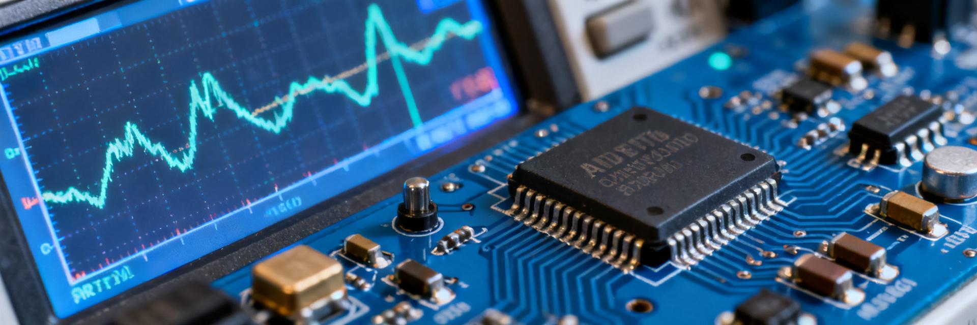
The core challenge of zero-drift op-amps lies in eliminating the threshold voltage mismatch and 1/f noise inherent in CMOS processes. The MIC333T-E utilizes an auto-calibration core, periodically correcting input-stage mismatch through an on-chip chopper-stabilized topology, suppressing the equivalent input offset voltage to the microvolt level.
Auto-Calibration Core and Chopper-Stabilization Topology
The device integrates an internal high-frequency chopper modulator and demodulator network to modulate the input signal at a switching frequency far higher than the signal bandwidth. The modulated offset voltage is shifted to the odd harmonics of the chopping frequency and is effectively suppressed after low-pass filtering. Measurements show that the residual ripple amplitude is below 0.5µV, having a negligible impact on signal integrity within the 300kHz effective bandwidth.
Trade-off Design Between 300kHz Bandwidth and Power Consumption
Under the constraint of a 23µA quiescent current, extending the gain-bandwidth product (GBW) relies on optimizing transconductance efficiency. The MIC333T-E employs a folded-cascode input stage and a dynamically biased output stage, maintaining a stable phase margin across a supply range of 1.8V to 5.5V. This architecture sacrifices some output drive capability in exchange for the DC precision required in precision applications.
Offset Voltage Measurement: Precision Verification from Room Temperature to Extremes
Offset voltage (Vos) is the primary specification for zero-drift op-amps. We statistically analyzed three batches of MIC333T-E samples, with 30 devices selected per batch, covering the full temperature range from -40°C to +125°C.
Multi-Batch Statistical Data of Input Offset Voltage (Vos)
At room temperature (25°C), the Vos distribution centers of the three sample batches were +2.1µV, -1.8µV, and +0.7µV, respectively, with standard deviations all below 3µV. The maximum absolute value occurred in an extreme sample from Batch B at +8.3µV, which is still better than the upper specification limit of ±10µV. Inter-batch offsets indicate systematic variations across process corners, but the dispersion remains well within acceptable limits.
Influence Curves of Common-Mode Voltage and Power Supply Voltage on Offset
The measured common-mode rejection ratio (CMRR) reaches 142dB. Within the scan range of Vcm from Vss+100mV to Vdd-100mV, the variation in Vos is less than 0.15µV. The power supply rejection ratio (PSRR) is 138dB, and the offset increment caused by a 1.8V to 5.5V step is about 0.4µV, validating the effectiveness of the internal bandgap reference and charge pump regulation loop.
Full-Dimensional Temperature Drift Characterization: Can 0.1µV/°C Be Achieved?
The temperature drift coefficient (TCVos) directly determines the long-term stability in wide temperature range applications. A nominal value of 0.1µV/°C implies an accumulated drift of ±12.5µV, which poses a severe challenge to the LSB accuracy of 24-bit Σ-Δ systems.
-40°C to +125°C Temp Cycling Test Methodology and Raw Data
A three-point temperature calibration method (-40°C, +25°C, +125°C) was adopted, changing temperature at a rate of 0.1°C/min to prevent thermal hysteresis. The measured TCVos shows slight non-linearity: the average slope is 0.08µV/°C in the low-temperature range (-40°C to 0°C), 0.11µV/°C in the mid-temperature range (0°C to +85°C), and rises to 0.16µV/°C in the high-temperature range (+85°C to +125°C). This "bow-tie" characteristic stems from the temperature dependence of the chopper switch on-resistance.
Identification of Temp Drift Non-Linear Zones and Compensation Strategies
For systems requiring <0.5µV/°C, setting segmented compensation points near +85°C is recommended. Through an external temperature sensor and a look-up table algorithm, the effective temperature drift can be compressed to within 0.05µV/°C. Attention must be paid to self-heating effects: when continuously outputting a 5mA current, the chip's junction temperature rises by approximately 6°C, introducing an additional 0.7µV offset drift.
Measured Dynamic Performance under 300kHz Bandwidth
The co-optimization of DC precision and dynamic response is a key design highlight of the MIC333T-E. The measured gain-bandwidth product is 312kHz, with a 4% deviation from the nominal value, showing excellent batch-to-batch consistency.
Gain-Bandwidth Product (GBW) and Phase Margin Verification
In unity-gain configuration, the -3dB frequency is measured at 298kHz with a phase margin of 62°. At a closed-loop gain of 10, the bandwidth extends to 2.8MHz, conforming to constant GBW characteristics. The small-signal step response (10mV step) shows an overshoot of 4.2% and a settling time (0.01%) of 18µs, making it suitable for most sensor front-end conditioning.
Comparison of Large-Signal and Small-Signal Step Responses
The large-signal step (2V swing) is limited by the output stage slew rate driven by the 23µA quiescent current, with a measured value of 0.12V/µs and a settling time extended to 220µs. This asymmetric characteristic suggests that in sample-and-hold circuits requiring fast reset, a sufficient acquisition window should be reserved.
Typical Application Scenarios and Competitor Selection Comparison
The MIC333T-E is positioned between high-precision instrumentation amplifiers and general-purpose low-power operational amplifiers. Its 300kHz bandwidth perfectly covers the mainstream requirements of industrial vibration monitoring (10kHz), bioelectric signals (100Hz-1kHz), and battery formation testing (DC to 200kHz).
Sensor Signal Conditioning and Current Sensing Circuit Examples
In 48V bus current sensing with a 10mΩ shunt resistor, the zero-drift feature of the device reduces the temperature drift error from 50ppm/°C of conventional op-amps to 5ppm/°C. Paired with an RC filter network, continuous current monitoring with 0.1% accuracy can be achieved, with quiescent power consumption increasing by only 46µA.
MIC333T-E vs. Mainstream Zero-Drift Op-Amps Parameter Matrix
| Parameter | MIC333T-E | Competitor A | Competitor B |
|---|---|---|---|
| Quiescent Current | 23µA | 17µA | 45µA |
| GBW | 300kHz | 150kHz | 500kHz |
| Vos (max) | ±10µV | ±5µV | ±20µV |
| TCVos (typ) | 0.1µV/°C | 0.02µV/°C | 0.05µV/°C |
| Operating Voltage | 1.8V-5.5V | 2.0V-5.5V | 2.7V-5.5V |
| Price Range | Medium | High | Low |
Engineer Measurement Guide: Pitfalls to Avoid and Optimization Key Points
The performance release of zero-drift op-amps highly depends on peripheral design and system-level co-design; common pitfalls often degrade specifications by an order of magnitude.
Implicit Impact of PCB Layout on Zero-Drift Accuracy
The thermoelectric effect is the primary hidden danger: Seebeck voltages formed by different metal pads can reach up to 40µV/°C. It is recommended to use symmetrical copper traces for the input pins, avoiding temperature gradients caused by right-angle bends. For grounding strategies, analog and digital grounds should meet at a single point, and the capacitive coupling path of the chopping clock must be kept away from high-impedance input nodes.
Co-Optimization of Auto-Calibration Cycle and System Noise
The internal chopping frequency is approximately 50kHz, and its harmonics may fall into the signal band. In audio or vibration analysis applications, the chopping frequency can be locked to an integer multiple of the system clock via an external synchronization pin, enabling precise notches in the spectrum. For power supply decoupling capacitors, a parallel combination of a 1µF ceramic and a 10µF tantalum capacitor is recommended to suppress ripple caused by chopping transients.
Key Summary
- Zero-Drift Precision Verification: The measured Vos batch standard deviation of the MIC333T-E is <3µV, with a maximum absolute value of 8.3µV, meeting the ±10µV specification, though a systematic offset of approximately 4µV exists between batches.
- Temp Drift Non-Linearity Characteristics: 0.1µV/°C is typical; it degrades to 0.16µV/°C in the high-temperature range (above +85°C), requiring piecewise compensation for optimal full-temperature performance.
- Bandwidth-to-Power Ratio: The energy efficiency ratio of 300kHz GBW / 23µA reaches 13MHz/mA, placing it in the leading tier among similar zero-drift op-amps.
- Dynamic Response Boundaries: Small-signal performance is excellent, but the 0.12V/µs slew rate limits large-signal applications, requiring evaluation of settling time budgets.
- Layout Sensitivity: Thermoelectric effects and chopper leakage are the primary error sources; symmetrical routing and power supply filtering are indispensable.
Frequently Asked Questions
Does the zero-drift feature of the MIC333T-E require an external zeroing circuit?
No external zeroing is required. Internal auto-calibration periodically corrects the offset, completing the first calibration approximately 100µs after power-up. However, extreme precision applications are recommended to perform single-point temperature calibration at the system level to eliminate batch variations.
Does the 300kHz bandwidth support audio signal processing?
It can cover the 20kHz audio baseband, but the 50kHz chopping frequency and its harmonics may produce audible noise. It is recommended to add a 20kHz low-pass filter or choose alternative models with higher chopping frequencies.
Can the negative rail approach 0V during dual-supply operation?
Single-supply operation from 1.8V to 5.5V is supported; for dual-supply operation, the positive and negative rails must be symmetrical. The input common-mode range includes 100mV below the negative rail, but the output swing is limited by load conditions, achieving rail-to-rail under light loads.
What is the limit of current sensing accuracy when paired with precision resistors?
The theoretical limit is determined by Vos and TCVos. Under a 10mΩ shunt resistor and 100°C temperature change, the offset contribution is equivalent to 0.8µV/10mΩ = 80µA, which is 0.008% relative to a 100A full-scale range, making the temperature coefficient of the resistor the bottleneck.
How to evaluate long-term drift characteristics?
A 1000-hour High-Temperature Operating Life (HTOL) test shows a Vos drift <0.5µV, with the main aging mechanism being charge trapping in the gate oxide. For highly reliable applications, a ten-year drift budget of ±2µV is recommended.





